
Decomposing Systolic Arrays

Systolic arrays are a recent innovation in chip architecture that accelerate matrix multiplications, making the most computationally expensive part of using and training LLMs significantly more efficient. Therefore, I think it’s important to understand how exactly they work.
Basics of Machine Learning
To motivate the need for systolic arrays, I want to quickly establish the basics of machine learning. At the most fundamental level, neural networks are composed of
where W is the weights matrix, x is the input matrix, and B is the bias matrix. I’ll save the details of what these mean and how exactly neural networks work1, but the large majority of the calculations that happen when a model is inferenced2 are y = Wx + B.
In terms of computational expense, the “+B” is trivial, as it’s an element-wise operation which can be computed at the same time for all elements. The W * x on the other hand requires multiple consecutive operations for a single output, so when broken down, most of the time during inference is used to perform
Now that I’ve established this, I can move onto how this calculation is computed in different types of chips.
Digital Logic Fundamentals
At the lowest level, computers are entirely composed of bits. Every single cursor movement, keyboard input, and operation performed on your computer is processed in 0s and 1s. These bits are updated every clock cycle (an arbitrary chunk of time). Each clock cycle is usually measured in nanoseconds, depending on your processor’s speed. For example, a 3GHz processor has a clock cycle time of 0.33 nanoseconds. A computer screen for example is refreshed in nanoseconds, which can’t be noticed by the human eye, but allows for the bits to refresh based on your movements and inputs.
Depending on the type of chip, the number of matrix multiplications that can be performed in one clock cycle greatly varies:
CPUs (central processing unit) have 4-8 cores and perform operations sequentially. Each core can execute a thread independently, which is a set of instructions. This makes CPUs great for executing a wide variety of tasks that don’t require a large number of computations per second, such as running any application on your computer, which entails many background tasks. Modern CPUs have combined multiply and add operations called FMA (fused multiply-add), which means they can perform both multiplication and addition in one clock cycle.
GPUs (graphics processing unit) have thousands of cores, but each core can only perform a few specific operations such as addition, multiplication, and subtraction. Essentially each core is a limited calculator. However, the lack of complexity makes them great for performing simple calculations in parallel. Each core can perform one FMA operation per clock cycle, making it significantly more efficient than a CPU.
A TPU (tensor processing unit) is a relatively newer chip, developed by Google to increase inference and training speeds. This chip was the first to bring the systolic array architecture, which was first introduced in 1982 paper by H.T. Kung, to modern chips. The systolic array takes 2*N - 1 + M number of clock cycles to compute the matrix multiplication of two matrices, where N is the number of columns and M is the number of rows in each matrix.3
Now let’s take a look at how long it would take for each of these chips to compute a 256x256 matrix multiplication, where both matrices are of the same dimensions.
A CPU can perform one FMA operation per clock cycle. A 256x256 matrix multiplication would have 16.7 million FMA operations, meaning it would take any modern CPU 16.7 million clock cycles to compute the product.
A GPU can perform FMAs in parallel. To keep it fair, let’s use a GPU that was comparable to the TPUv14 : NVIDIA’s K80 GPU, which has around 2500 cores. Since each core can perform one FMA per clock cycle and there are 2500 cores, it would take 16.7M/2.5k = 6.7k clock cycles for the GPU to compute the output matrix.
A TPU can compute the output in 2*N - 1 + M clock cycles, where N and M are both 256 in this case. This means it would take the TPU 511 clock cycles to compute the output.
The GPU is 2500x faster than the CPU and the TPU is 13x faster than the GPU, making it approximately 32500x faster than the CPU. More notably, this difference grows exponentially relative to the the size the arrays being multiplied. Clearly this is a large increase in efficiency. Now that this has been established, let me explain how systolic arrays actually work.
Understanding Systolic Arrays
TPUs have several improvements over GPUs, mainly dealing with faster on-chip memory, but the most significant difference in terms of architecture is the implementation of systolic arrays in TPUs.
 | Google Cloud Blog")
Although the diagram above seems complicated, the matrix multiply unit (MMU) is what performs most of the computation. Unsurprisingly, this is where the systolic array is located.
When viewed as an abstraction, the MMU takes in a set of 2 inputs (weights and input activations) and produces outputs. A systolic array is composed of individual elements called processing elements (PE). Each PE performs the same task: multiply and accumulate. In functionality they’re quite similar to GPU cores. However, what separates the systolic array is how the data moves through these “cores”. All adjacent cores are connected with wires, which removes any overhead in deciding where the data should progress next. Each clock cycle, the inputs move to the right and the accumulated sums move to the bottom. The accumulated sum is either a product (on the first row), the sum of several products (after the first row). Here’s a clear illustration of the data movement:
Initially, the weights are loaded into the PEs and remain stationary during the entire matrix multiplication.
The inputs are loaded in from the left, but in a staggered format.
Essentially, each consecutive row is delayed by 1 clock cycle. If you had a 3x3 matrix, the first input from the third row would be under the element X22. The reason for this is simply because the math just works out this way. If all inputs were fed in simultaneously, X1 would be added with X2, which is mathematically incorrect.
Now let’s walk through what happens on each clock cycle.
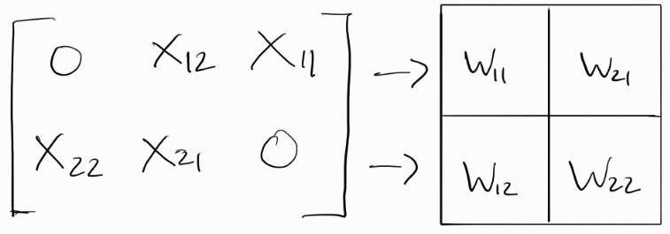
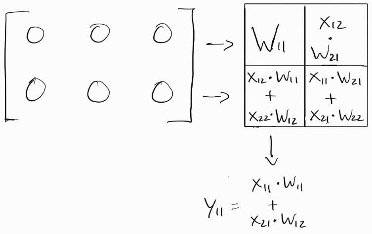
Clock Cycle 1:
X11 moves right to to PE1, which is holding W11. X11 and W11 are then multiplied:
Notice how all of the inputs, even within the input matrix moved to the right. This happens every clock cycle.
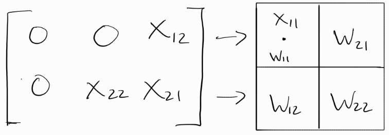
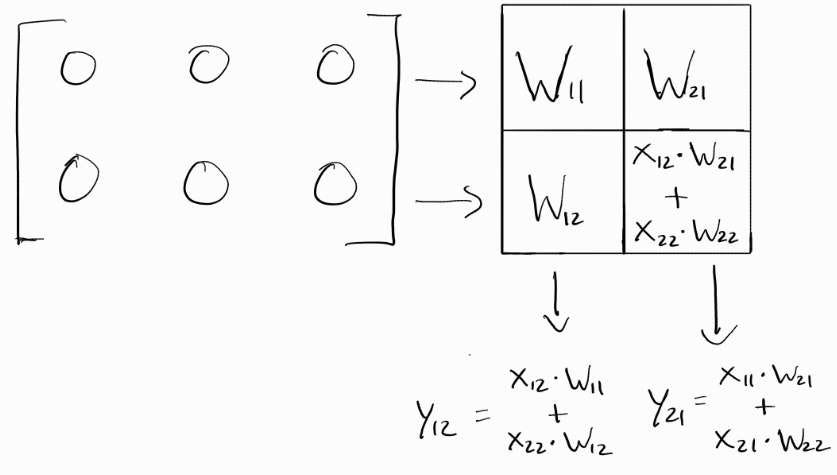
Clock Cycle 2:
X11, X12, and X21 move to the right and X11*W11 moves down.
As expected, all inputs moved to the right. X11*W11 was an accumulated sum, which is why it moved down.
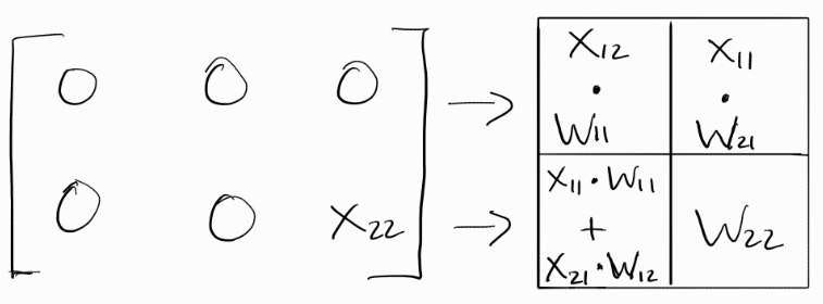
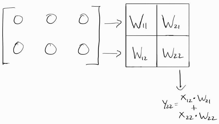
Clock Cycle 3:
All of the inputs move to the right once again and the accumulated sums move down. In this case, since (X11*W11 + X21*W12) was already in the lowest row, it simply goes into the output matrix. If this was a 3x3 matrix, the next row would have an accumulated sum of 3 products.
Clock Cycle 4:
Once again, the inputs move to the right and the accumulated sums from the previous cycle become outputs, as they’re already on the lowest row.
Clock Cycle 5:
Finally, the accumulated sum from the last clock cycle moves down to become an output.
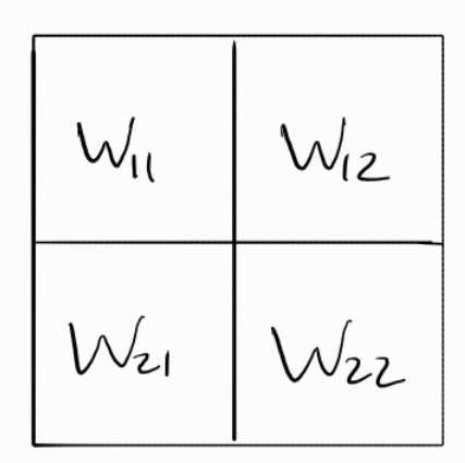
The final output matrix will look like this:
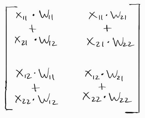
This matches the manual calculation I did.
All PEs operate exactly like this - they follow the principle of inputs moving to the right and accumulated sums moving down.
Closing Notes
I want to note that what I discussed above was a type of systolic array called weight-stationary systolic array, meaning the weights stay in place. There is another type called non-weight-stationary systolic array, which I decided not to cover, as weight-stationary is the industry standard and considered better due to several reasons, which you can read more about here.
If you understood that, you just learned the inner workings of the chips that will power the next generation of tech. Very fascinating to think about how complex math can be reduced down to repetition of patterns. If you enjoyed this and want to learn more, I highly recommend checking out this article, as it goes deeper into the nuances of systolic arrays.
If you’re interested in how a systolic array can be designed in code, you can find my Verilog implementation here.
Inference is the general term for using a model after it’s trained. For example, when you use ChatGPT, you’re inferencing GPT-4.
Note that for a matrix multiplication to be mathematically computable, the number of rows in the first matrix has to equal the number of columns in the second matrix.
For context, Google’s currently on TPUv6 and current commercial state-of-the-art GPUs such as the RTX 5090 have up to 25,000 cores.